- Home
- Experiment Data
Experiment Data
-

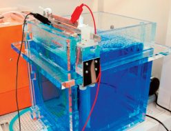
Achieved a film thickness distribution of ±3-5% or less compared to the target film thickness of 3 μm. Example of copper sulfate plating test results
Our plating equipment for silicon wafers has been introduced in many universities and research institutes, and here we introduce data from actual experiments conducted using the equipment. This time, the standard equipment for 8-inch wafers was used, and the target film thickness was 3 μm.
Read more