- Home
- Experiment Data, Wafer
- Achieved a film thickness distribution of ±3-5% or less compared to the target film thickness of 3 μm. Example of copper sulfate plating test results
TECHNICAL INFORMATION
Achieved a film thickness distribution of ±3-5% or less compared to the target film thickness of 3 μm. Example of copper sulfate plating test results
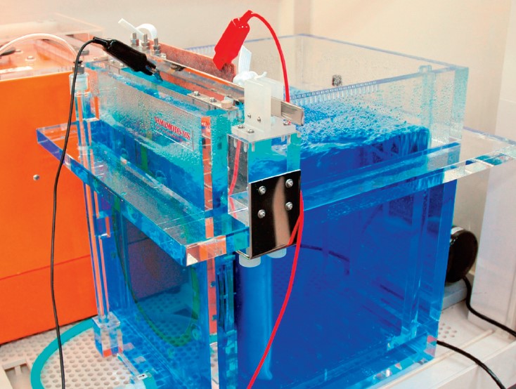
Our plating equipment for silicon wafers has been introduced in many universities and research institutes, and here we introduce data from actual experiments conducted using the equipment.
This time, the standard equipment for 8-inch wafers was used, and the target film thickness was 3 μm.
〇Equipment used
A-52 SILICON WAFER PLATING LABORATORY EQUIPMENT SET
Programmable Power Supply YPP15100WA
〇Experimental condition
| Plating bath | Cu-sulfate electroplating solution with commercial additives |
| Sample | 8inch Wafer with sputter-deposited Cu film |
| C.D | 1A/dm2 |
| Target thickness | 3 μ m |
| Anode | Phosphorus Copper |
| Bath Temp | R.T. (25ºC ± 1ºC) |
| Agitation | Air bubbling, Paddle agitation |
〇Sample Specification
| Sample Size | 8inch Silicon Wafer Test Piece |
| Pattern and wafer specification | Octagonal/square line (Spiral pattern) |
| L/S | 5 – 100 μm |
| Round/Square Bump, Diameter | 10 – 500 μm |
| Wafer thickness | 725 μm |
| Sputter-deposited Cu | 300nm |
| Resist thickness | 5 μm |
〇Sample Appearance / State after plating
Upper left: Wafer appearance / Upper right: Enlarged pattern
Lower left: Film state in the center of the pattern (3D) / Lower right: Enlarged view of the film state in the center of the pattern
〇Sampling points
After plating, we measured the plating film thickness at the following 9 points.

Plating film thickness measurement results
The plating film thickness values for each sample point are as follows. Film thickness distribution of ±3-5% or less is achieved for a plating target of 3 μm.
| Sample Points | □40μm | □100μm |
|---|---|---|
| a | 3.012 | 3.006 |
| b | 3.006 | 2.934 |
| c | 3.036 | 2.857 |
| d | 2.959 | 2.871 |
| e | 3.189 | 3.026 |
| f | 3.191 | 3.023 |
| g | 2.961 | 2.975 |
| h | 2.929 | 2.867 |
| i | 3.072 | 2.856 |
| Ave | 3.039 | 2.935 |
| Max | 3.191 | 3.026 |
| Min | 2.929 | 2.856 |
| Ran | 0.262 | 0.170 |